PCB stack-up of 8-layer test board

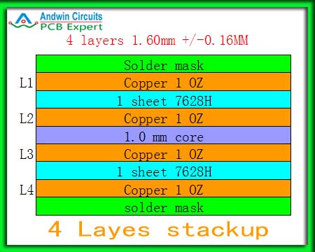
PCB stack up - Andwin Circuits

4 Layer PCB Layout Tutorial, Stack-up design, and Cost of manufacturing - Absolute Electronics Services

Temperature-time histories of the RF heated raisins (to a center

Designing a 6-Layer PCB Stackup for Enhanced EMC, Blog
PCB Layer Stackup, PCB Stackup Design

PCB stack-up of 8-layer test board

Simulated (LLLE x Kopelman) temperature (°C) profiles of raisins

Targets are modeled as entering at locations p1, p2, …, p4 at the

/wp-content/uploads/2023/10/PCB-8-Layer
Stuck Designing Two-Layer PCBs? Give Four Layers A Try!

Targets are modeled as entering at locations p1, p2, …, p4 at the