Latest advance on seamless metal-semiconductor contact with

RF CMOS Technology Introduction, Advanced PCB Design Blog
Manufacturing quality through semiconductor packaging design
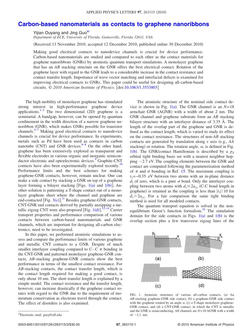
PDF) Carbon-based nanomaterials as contacts to graphene nanoribbons
Scientists revolutionize wireless communication with three
Scientists revolutionize wireless communicati

Nano Today, Vol 42, February 2022
ELNES at the 1T /2H-MoTe 2 boundary. (a) A HAADF image showing the

Atomic-Scale Structure of Mo6S6 Nanowires
PDF) Black Phosphorus Nanosheets in Field Effect Transistors with Ni and NiCr Contacts
How are Semiconductors Made? A Comprehensive Guide to Semiconductor Manufacturing
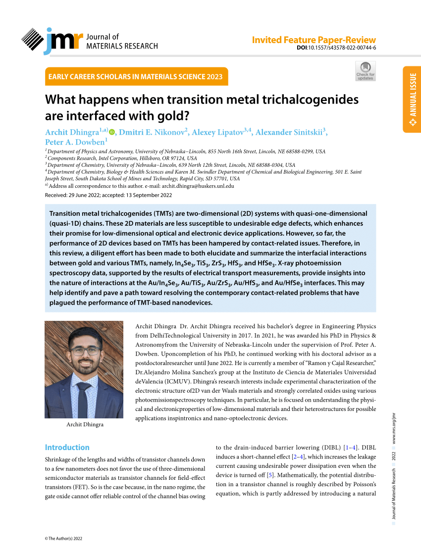
PDF) What happens when transition metal trichalcogenides are interfaced with gold?
MPW Service, Foundry
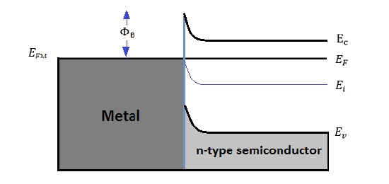
Metal-Semiconductors Contacts - Engineering LibreTexts
Transition from Schottky to Ohmic contacts in 2D Ge/GaAs heterostructures with high tunneling probability - Physical Chemistry Chemical Physics (RSC Publishing) DOI:10.1039/D3CP06189B

ELNES at the 1T /2H-MoTe 2 boundary. (a) A HAADF image showing the